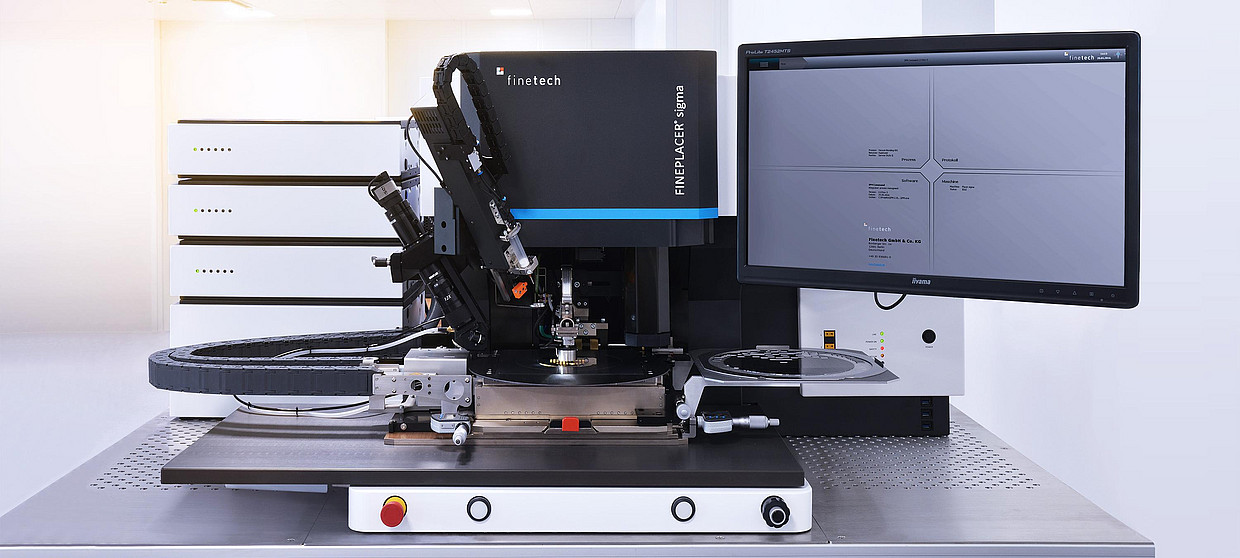
FINEPLACER® sigma
- Categories: R&D Bonders, Uncategorized
- Manufacturer: Finetech

Advanced Sub-Micron Bonder
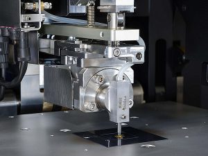
The FINEPLACER® sigma combines sub-micron placement accuracy with a 450 x 150 mm working area and bonding forces up to 1000 N.
The system is ideal for all types of precision die bonding and flip chip applications at chip and wafer level. This includes complex 2.5D and 3D IC packages, Focal Plane Arrays (i.e. image sensors), MEMS/MOEMS, and more.
Placing small devices on large substrates is made possible by the FPXvisionTM optical system design. With this alignment system, the smallest structures at the highest magnification can be viewed across the entire field of view. Moreover, FPXvisionTM introduces pattern recognition to a die bonder with manual alignment.
The FINEPLACER® sigma embraces all features of an assembly and development platform capable of handling an unlimited spectrum of applications and prepared for future technologies.
About the FINEPLACER® sigma
"We use the FINEPLACER® sigma for a variety of applications, ranging from simple chip-to-submount to complex module assemblies with very high accuracy requirements. Easy manual operation makes the system also an ideal fit for low-quantity research samples." Lars Schellhase Ferdinand-Braun-Institut Key Facts* Large bonding area Reproducible sub-micron placement accuracy Pattern recognition for software verified alignment Wide range of supported component sizes UHD vision alignment system with FPXvisionTM Modular machine platform allows in-field retrofitting during entire service life Wide range of component presentation (wafer, waffle pack, gel-pak®) Synchronized control of all process related parameters Process module compatibility across Finetech platforms Individual configurations with process modules Ultra low bonding force Data/media logging and reporting function Wide range of controlled bonding forces In-situ process observation in HD Full process access & easy visual programming with touch screen interface Numerous bonding technologies (adhesive, soldering, thermocompression, ultrasonic) 3-color LED illumination Sequence control with predefined parameters *depending on configuration Applications & Technologies With a broad range of supported applications and technologies, our die bonding systems are ready to tackle any application challenge in the industry. And as market requirements shift and new technologies emerge, their modular hardware and software architecture ensures maximum technological versatility over the entire service life. Micro-optical bench assemblyIR detector assemblyGas pressure sensor assemblyVCSEL/photo diode (array) assemblyVisual image sensor assemblyGeneric MEMS assemblyMicro optics assemblySingle photon detector assemblyUltrasonic transceiver assemblyLaser diode assemblyµLED (array) assemblyLaser diode bar assemblyHigh-power laser module assemblyAcceleration sensor assemblyGeneric MOEMS assemblyInk jet print head assemblyX-ray detector assemblyOptical sub assembly (TOSA/ROSA)E-beam module assemblyMechanical assembly Adhesive bondingThermocompression bondingThermo-/ ultrasonic bondingSoldering / eutectic solderingSinteringPrecision vacuum die bonding Chip on Flex/Film (CoF)Chip on Glass (CoG)Multi chip packaging (MCM, MCP)Flip chip bonding (face down)2.5D and 3D IC packaging (stacking)Wafer level packaging (FOWLP, W2W, C2W)Precision die bonding (face up)Flex on boardChip on board (CoB) Functions - Modules - Enhancements Our die bonding solutions are as individual as our customers' requirements and offer a wide range of configuration options. In addition to the system's basic functions, which are part of the standard functional range, numerous process modules are available for each system, expanding the spectrum of applications. Retrofittable at any time, they enable additional die bonding technologies and processes either directly or as part of a module package. A selection of functional enhancements and accessory systems make daily work with the die bonder easier and help to make certain technology and process sequences even more efficient.
Focal Plane Array / IR Sensor Assembly
A Focal Plane Array (FPA) is a sensor with a two-dimensional detector pixel matrix, i.e. for infra-red light or X-rays, positioned in the focal plane of an optical system.
Eutectic Bonding with Au/Sn
Eutectic Gold/Tin (Au/Sn) is a hard solder alloy often used to bond demanding microelectronic and optoelectronic devices. They are available in different forms, such as pre-forms, solder paste or ribbons.