FINEPLACER® lambda 2
- Categories: R&D Bonders, Uncategorized
- Manufacturer: Finetech
Sub-Micron Table Top Die Bonder
The all-new table top flip chip bonder FINEPLACER® lambda 2 builds on its acclaimed predecessor to set new standards in precision die attach and advanced chip packaging for opto-electronic assemblies and more.
The completely revised table top die bonding platform can be easily configured for a wide range of applications for process development or prototyping. Numerous process module options and in-field-retrofit capabilities guarantee maximum technological flexibility of the table top die bonder to protect your investment in the face of ever-changing challenges.
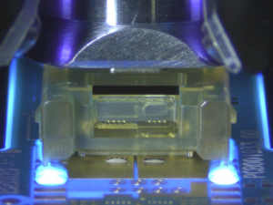
Due to the table top flip chip bonder’s ergonomic machine design and software-supported user guidance, the user remains at the center of action. Powerful optical systems allow the user to keep an overview at all times, even when working in the sub-micron range.
The table top die bonder FINEPLACER® lambda 2 shares a common module range and innovative operating software with Finetech’s automatic die bonding systems to ensure a seamless process migration to series production. Ask us about our scalable solutions.
About the FINEPLACER® lambda 2
We use the FINEPLACER® lambda 2 for development processes on MEMS, e.g. for precise dispensing and the placement of microstructures. The system fits in with the investment strategy at ISS, where flexible facilities with a wide range of materials enable research into new materials and, in particular, rapid prototyping. Going forward, this will enable us to develop new capabilities for our customers' ideas at an even faster rate.Severin Schweiger, Fraunhofer IPMS, Integrated Silicon Systems
Key Facts*
- Sub-micron placement accuracy
- Superior optical resolution
- Excellent price performance ratio
- Fully manual or semi-automatic machine versions
- Individual configurations with process modules
- Numerous bonding technologies (adhesive, soldering, thermocompression, ultrasonic)
- Data/media logging and reporting function
- Wide range of controlled bonding forces
- Full process access & easy visual programming with touch screen interface
- Various bonding technologies in one recipe
- Process module compatibility across Finetech platforms
- In-situ process observation in HD
- Modular machine platform allows in-field retrofitting during entire service life
- Synchronized control of all process related parameters
- Overlay vision alignment system (VAS) with fixed beam splitter
- Sequence control with predefined parameters
Applications & Technologies
Chip on Flex/Film (CoF)Flip chip bonding (face down)2.5D and 3D IC packaging (stacking)Precision die bonding (face up)Chip on Glass (CoG)
Functions - Modules - Enhancements
Our die bonding solutions are as individual as our customers' requirements and offer a wide range of configuration options. In addition to the system's basic functions, which are part of the standard functional range, numerous process modules are available for each system, expanding the spectrum of applications. Retrofittable at any time, they enable additional die bonding technologies and processes either directly or as part of a module package. A selection of functional enhancements and accessory systems make daily work with the die bonder easier and help to make certain technology and process sequences even more efficient.Technical Paper
VCSEL Bonding
The packaging of opto-electronic units is one of the key applications of Micro Assembly. Highly dense packaged multiplex transmitters, receivers and combined assemblies are...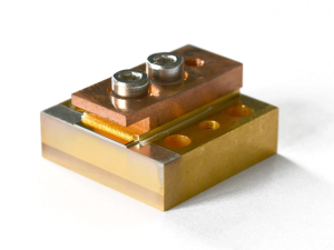
VCSEL Bonding
Semiconductor Laser diode bars are high power products, used in places where small and efficient emitting light sources are needed. Primarily, these Lasers are being used as pumping sources for optical resonators of solid state Lasers or gas Lasers.