


Multilayer PCB Reverse Engineering System – ScanFAB™
- Category: PCB Reverse Engineering, Redesign, & Repair Software
- Manufacturer: ScanCAD

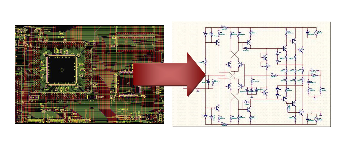
A fully integrated, stand-alone, scanner- based re-engineering system that permits the creation of CAD data (DXF/Gerber/Drill/CNC) from existing multilayer PCBs, parts, phototools, stencils, drawings, microfiche, PDF files, X-Ray images, etc. It contains a full Gerber editor that can be used to import, modify and export Gerber & Drill data.
About the Multilayer PCB Reverse Engineering System – ScanFAB™
Why use ScanFAB?
- NECESSITY - Create high quality CAD data for legacy products that are required for PCB fabrication, test and repair.
- ACCURACY - Extracted data is exact Form, Fit and Function, eliminating need to re-certify & perform compliance and environmental testing. (UL, CE, EMI, SI, etc.)
- QUALITY - Increase data quality by using internal Quality Check features
- SECURITY - Prevent PCB/film/drawing deterioration by storing images in digital format
ScanFAB uses Windows-based software linked to a high-resolution, calibrated flatbed scanner. This combination allows for accurate reverse engineering and precise reproduction of data to exact FORM, FIT and FUNCTION for today's high density PCB board designs, complex parts and tooling.
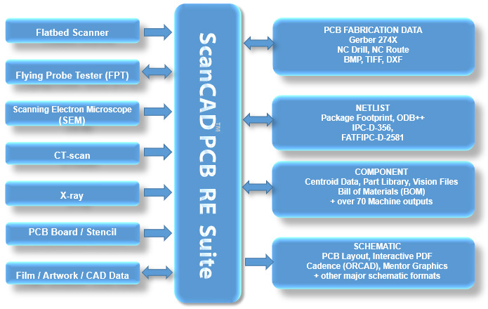
Simple Process Flow
The process of image capturing for all PCB layers is done in Color, Gray or B&W. The conversion of Raster to Vector data is fully supported with numerous automatic functions. The Quality Check functions insure that the data is accurate and of good quality. Support materials include context sensitive help, videos and workflows.
Automatic Features
ScanFAB offers various functions to quickly and automatically "vectorize" the scanned image creating a digital twin:
- Flash Pads (circular, square, oval, rectangle)
- Tracks (orthogonal/all angle)
- Silkscreen, Soldermask
- Copper Fill Areas/Ground & Power Planes
- Crosshatched Areas (90°/45°)
- Stencil Files
- Pads and tracks on grid
- Step & Repeat
- Drill & Route CNC data
Verification
Worried about the quality of the finished CAD data? Use ScanFAB's "check functions" to verify the quality and accuracy of the data:
- Check Gerber vs scanned vs imported images
- Design and Clearance rule checks
- Delete “double-hit” pads
- Verify track & pad connections
- Check for potential shorts & opens
- Layer-to-Layer registration
- Manually modify data as needed (damaged PCB)
Scanning and Data Import
- Flex, Ceramic & FR4 substrates, film, paper
- Stencils, screens, diazo, silver, glass & chrome
- Single, Double & Multi-layer PCBs
- Verifiable image alignment & deskew
- Automatic layer-to-layer alignment
- Up to 99 layers in each job
- Gerber Data 274D & 274X
Output Files
- Gerber files (274X or 274D)
- Comprehensive aperture tables
- Drill files: Excellon, Sieb & Meyer
- Stencil files
- Soldermask, Padmaster, Silkscreen
- Circuit, Ground/Powerplane
- DXF
- BMP, TIFF images
- Panelized images